Overview
|
In this project we had to make an asynchronous counter that would count up to 80, pausing when it reached it, and then reset back to 0 at a switch.
|

|
Multisim Pictures & explanation

The PLD mode for the circuit
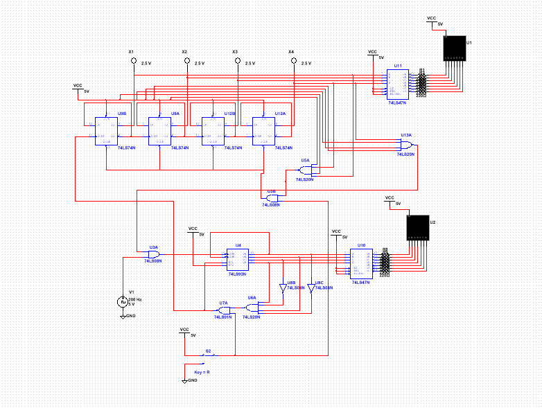
The Design mode for the circuit
In multisim there are 2 different "modes" you can use, PLD and Design mode. Design mode is the more commonly used version, that allows for easier testing by allowing seven segment displays and other similar screen items. PLD mode is where you build circuits that will be uploaded to a PLD or a programmable logic device. In PLD mode you place objects not by using the 74ls numbers on them, but their names. For example to place a double input and gate, you would place down AND2 instead of 74ls08. Also in PLD mode, you have to assign pins to certain things like switches and the clock power, so that when you breadboard the PLD device you can interact with your switches and have a clock source. There are 2 kinds of pin assignments, input and output connectors. Input connectors are what you assign to switches and sources, output connectors are what you assign to where you want to connect your seven segments that are on a seven segment display. To upload a design to the PLD, you plug it into the computer through a usb cable and click on transfer and then export to PLD.
Bill of Materials
Materials Quantity
PLD 1
Breadboard 1
wires 15
NI myNAQ 1
PLD 1
Breadboard 1
wires 15
NI myNAQ 1
Conclusion
During DE we have used 2 different types of integrated circuits, MSI and SSI. SSI, which stands for small scale integration, has fewer components than MSI, which stands for medium scale integration. SSI circuits utilize components like the 74ls93, which has the functionality of four flipflops in one device, where as MSI utilizes the individual 74LS74 flip flops. MSI devices do have limitations, such as not being able to set a lower limit, or count down. The "ripple effect" occurs in asynchronous counters and is a situation where the signals coming from the clock slowly distance themselves from each other in a ripple. In my circuit, the signal originates from the clock, which goes into an AND gate and into the 74ls93 chip. From there the 93 chip begins functioning like 4 flipflops and outputs four signals which feed into a 74ls74 and from there into a 7 segment display, making up the ones digit. From the four outputs of the 93, the LSB is put into an inverter, along with the second digit in from the MSB (0101), which are both put into a 4 input NAND along with the other 2 outputs. The output from that 4 input NAND gate goes into another 2 input NAND gate, along with a switch used to reset it. The outputs from that NAND gate go two places, the 93 chip to be able to reset it, and into the clock of the first 74LS74 flip flop. The NotQ on the first second and third flip flop are then fed into the clocks of the second third and fourth flipflops respectively. The D of the first second third and fourth flip flop are put into the NotQ of themselves. The 4 Q's are then put into another 74ls47 and again into a seven segment display to act as the 10s digit. The Q of the fourth flip flop is fed into 2,, 4 input NAND gates, one of them feeds into the first AND gate and will suspend the count at 80(the other inputs are VCC), another NAND gate (also has the Q from the first flip flop and the other inputs are VCC) is fed into an AND gate that is also being fed the rest switch. and the output of that AND gate is fed into the CLR's on all flip flops. Pressing the reset switch will then clear both displays at the same time. None of my classmates designs differed greatly from mine, but some had their count go up by the push of a button instead of automatically through a clock.
